Synthesizing and deploying SystemVerilog designs onto a Basys 3 with Vivado
Overview
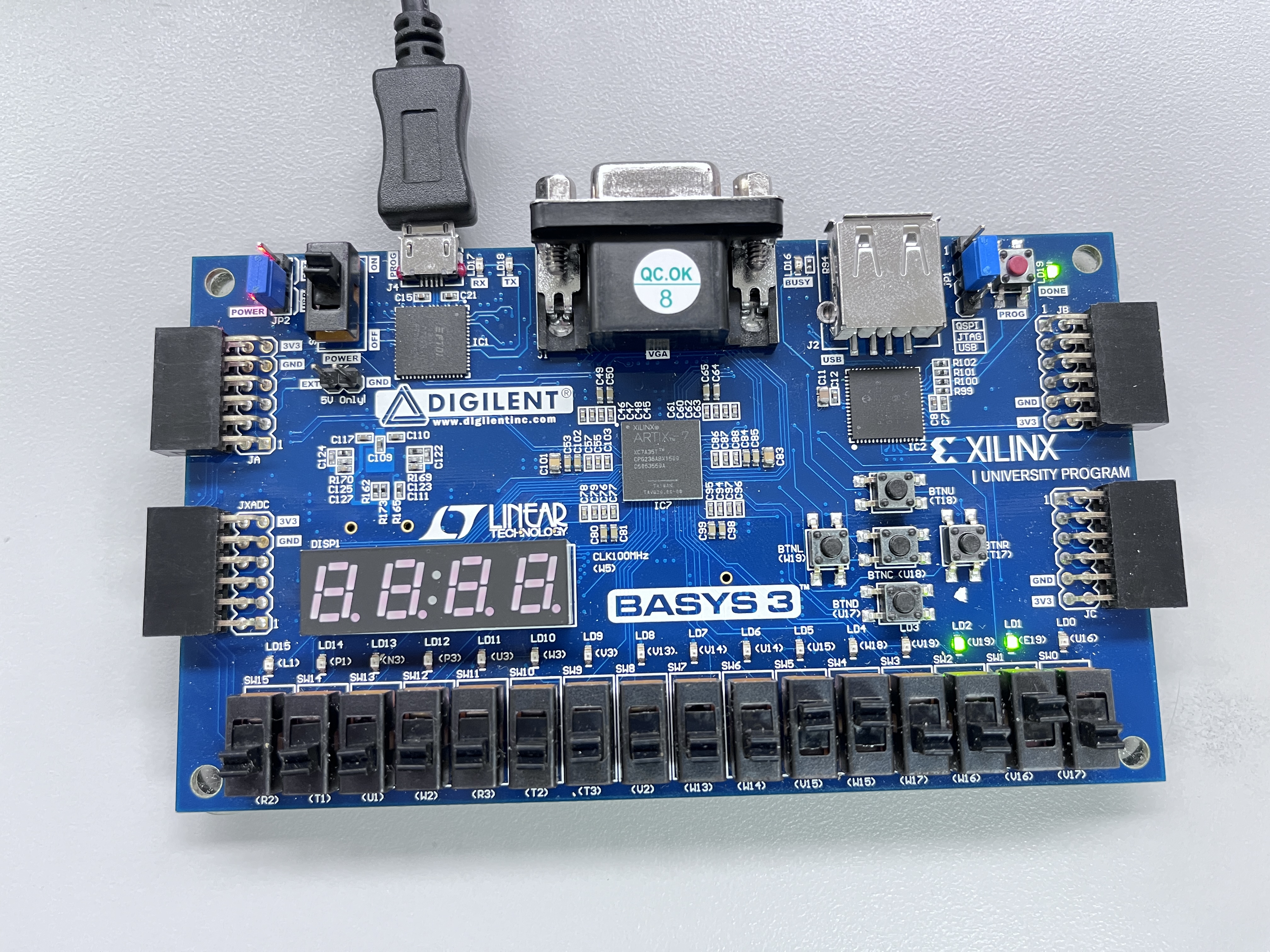
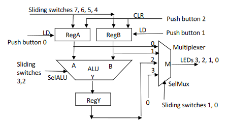
This project involved designing and implementing a 4-bit ALU circuit in SystemVerilog by integrating registers, a multiplexer, and an ALU core to perform arithmetic and logic operations. The design was synthesized and deployed on a Basys 3 FPGA using Vivado to ensure that it executes in real-time with hardware.
Design
The ALU circuit consists of:
- Three 4-bit registers for storing input and output values
- A 4-bit ALU module capable of performing:
- Addition
- Subtraction
- Bitwise OR
- Bitwise AND
- A 4:1 multiplexer, selecting between register outputs
- A clock-driven control system using FPGA buttons to manage data loading and operation selection
The design was written using behavioral modeling in SystemVerilog and synthesized in Vivado, ensuring correct functionality when deployed on the Basys 3 FPGA.
Implementation
- Designed and simulated the ALU and supporting modules in SystemVerilog
- Defined FPGA constraints to map inputs and outputs to LEDs
- Synthesized and implemented the design in Vivado
- Deployed the project onto the Basys 3 FPGA to verify real-time operation using hardware inputs and outputs
Results
Successfully demonstrated real-time ALU operations on the Basys 3 FPGA as correct results were displayed on the on-board LEDs
Future Improvements
- Expand ALU to include shift and XOR operations
- Extend registers to support larger bits
Further Information
More information will be provided in the lab report.